- HBM (High Bandwidth Memory) is the stacked-DRAM chip every modern AI accelerator needs — and the supply chain bottleneck that gates which GPUs ship and at what margin. Each NVDA Blackwell B100 ships with 192GB of it; each AMD MI350X ships with 288GB.
- Three companies make it, and the ranking reshuffled through 2025. SK Hynix leads (~50-62%); Micron (MU) overtook Samsung to take #2 (~21-25%); Samsung fell to #3 (~17-20%) on HBM3E qualification delays.
- Investor leverage doesn't sit only with NVDA — it sits across the cohort: MU (US-listed pure-play), TSM (CoWoS packaging is the second bottleneck after HBM itself), and the demand-side beneficiaries when hyperscaler capex guides go up.
Every NVDA H100 ships with 80GB of HBM. Every H200 ships with 141GB. Every Blackwell B100 ships with 192GB. Most of an AI chip’s bill of materials isn’t the GPU die itself — it’s the eight-high stack of memory sitting next to it. That stack is HBM memory (High Bandwidth Memory), the supply-chain bottleneck the AI infrastructure cycle quietly runs through. The HBM market landed around $35B in 2025 and is on track for ~$100B by 2028 per Introl analysis citing TrendForce — with Bank of America research via TrendForce pegging 2026 at ~$54.6B en route. Three companies make it. One company packages it. And the public-equity leverage isn’t where most retail investors think.
Micron (MU) — ticker above — last printed $681.54 going into publication on May 19, 2026. Its FY2025 Q4 earnings release (fiscal year ending August) showed HBM revenue reaching roughly $2B in Q4 alone on total revenue of $11.32B — and the data-center segment hit 56% of company revenue, with HBM as the leading component. That’s the US-listed pure-play angle this post will return to in the cohort section.
Why HBM Memory Matters Right Now
The short version is the memory wall. GPUs got 60–100× faster in raw FLOPS over the last decade. Conventional DDR DRAM only got roughly 3× faster in bandwidth over the same period. The gap is what makes modern AI training and inference bandwidth-bound, not compute-bound — feed the cores fast enough and they’re idle waiting for data.
HBM solves the wall by stacking DRAM dies vertically (8 or 12 dies high) on a silicon interposer right next to the GPU. A single HBM3E stack delivers ~1.2 TB/s of bandwidth versus ~38 GB/s for a DDR5 DIMM — roughly 30× the throughput per package, accessible to the GPU without leaving the silicon interposer.
That’s why every meaningful AI training run since GPT-4 (2023) has been bandwidth-bound, and why hyperscaler capex (MSFT / META / GOOGL / AMZN) is implicitly an HBM order book. When MSFT guides capex up 30% next quarter, that translates downstream into HBM allocations at SK Hynix, Micron, and Samsung. And the bottleneck isn’t theoretical — SK Hynix and Micron have been sold out through 2025 and most of 2026, with NVIDIA-class customers booking allocations years in advance.
How HBM Memory Actually Works
The physical stack: 8 or 12 DRAM dies stacked vertically, connected by Through-Silicon Vias (TSVs) — micro-holes drilled through the silicon that carry electrical signals between layers. Each stack sits on a logic base die that handles I/O. HBM3E generations come in two heights: 8-Hi (24GB per stack) and 12-Hi (36GB per stack, using the same 24Gb DRAM dies but stacking more of them).
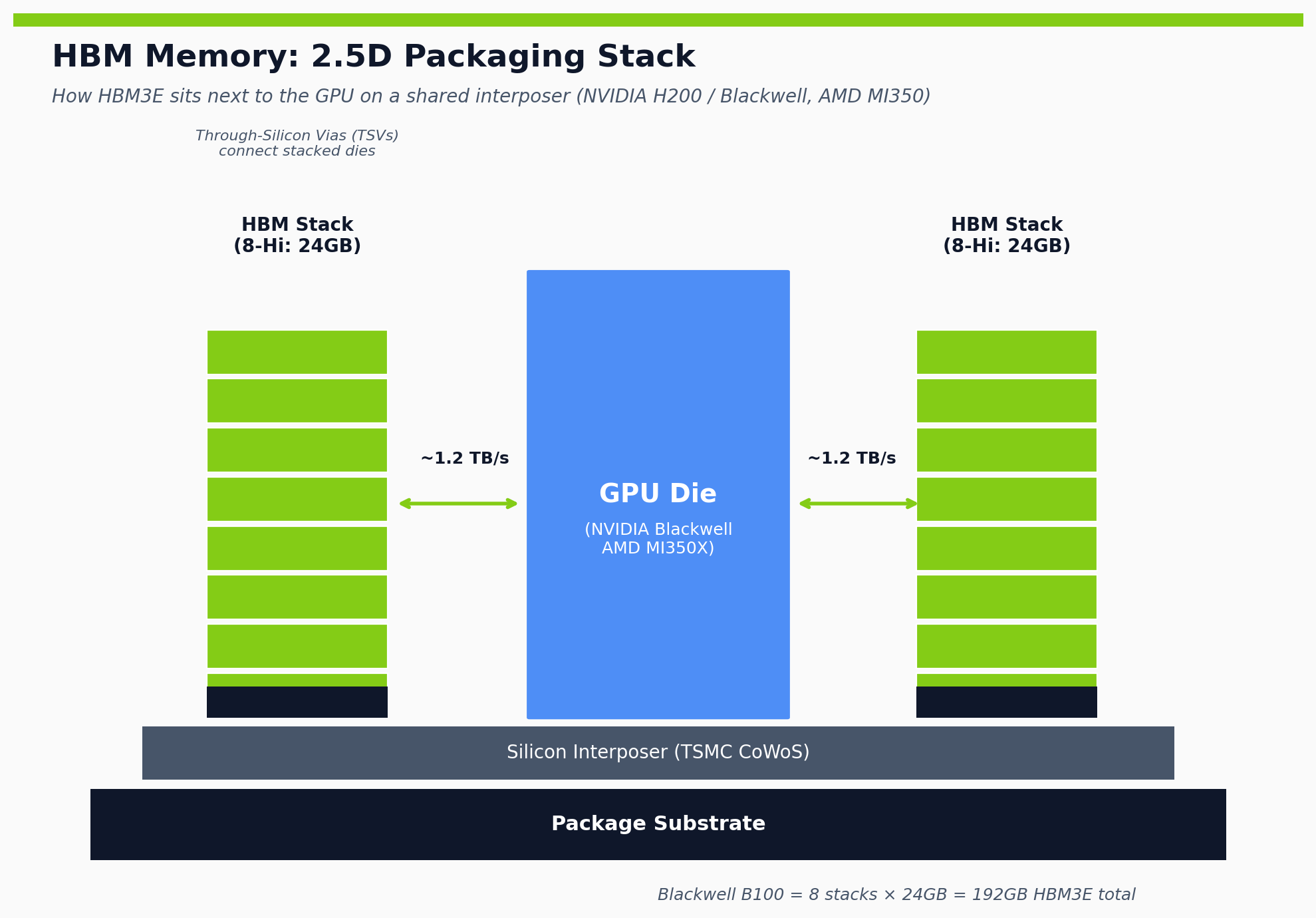
HBM stacks don’t go directly on the GPU board. They sit on a silicon interposer alongside the GPU die. This “2.5D” packaging is called CoWoS — Chip-on-Wafer-on-Substrate — at TSMC. Without CoWoS, an NVIDIA Blackwell GPU is just a collection of dies, not a finished product. Per multiple industry trackers, TSMC has booked ~50-60% of its CoWoS capacity to NVIDIA alone through 2027.
Generations matter for who’s competitive at any given moment. HBM2 → HBM2E → HBM3 → HBM3E → HBM4 — each generation roughly doubles bandwidth per stack. NVDA H100 uses HBM3. H200 and Blackwell use HBM3E. AMD’s MI350X uses HBM3E in 12-Hi configuration (288GB total on 8 stacks × 36GB). The future NVIDIA Rubin generation is expected to use HBM4, which SK Hynix has been first to mass production on.
Capacity per stack matters because of the math: Blackwell B100 = 8 stacks × 24GB = 192GB total HBM3E. AMD MI350X = 8 stacks × 36GB = 288GB total. On the latest generations, HBM dollar value is 40-50% of total GPU package cost. That’s not a side ingredient — it’s nearly half the chip.
Where the Money Flows — The HBM Cohort
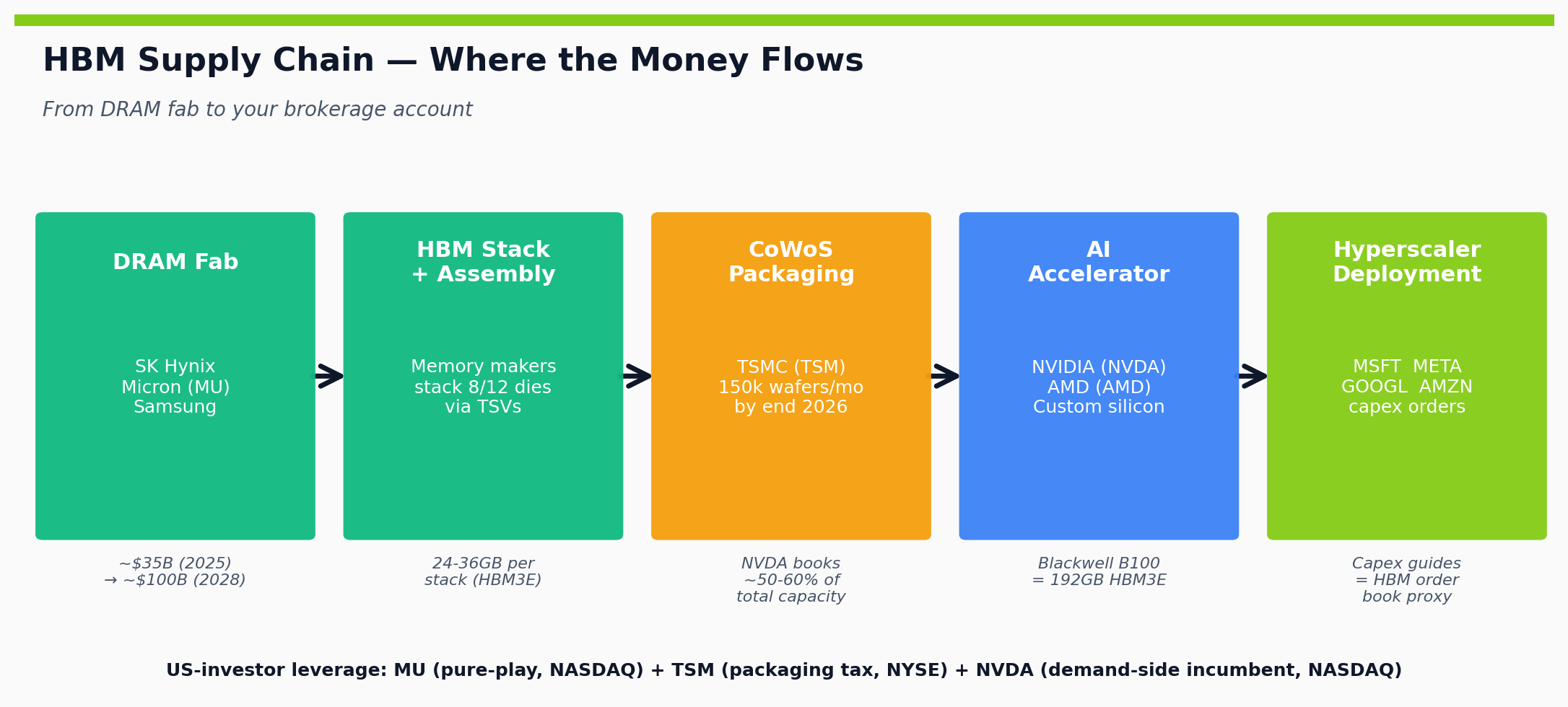
The investor-lens question is who profits when HBM demand keeps compounding. Three buckets matter.
The Big Three memory makers (~100% of the HBM market — but the ranking reshuffled through 2025):
- SK Hynix (Korea, KRX: 000660) — clear #1 with ~50-62% share, NVDA’s primary HBM3E supplier. The cleanest pure-play AI memory beneficiary, but US-investor access is via Korea ETFs (EWY, FLKR) or the Hynix ADR on OTC. First to mass-production on 12-Hi HBM3E.
- Micron Technology (MU) — now #2 at ~21-25% share. The only US-listed pure-play exposure in the cohort, and the one Wall Street uses when it wants direct HBM beta. HBM revenue hit ~$2B in fiscal Q4 2025 on total revenue of $11.32B — roughly 18% of the company. Note that Micron still has commodity DRAM exposure (PC, mobile, server DDR), so it’s not 100% HBM-leveraged, but the data-center segment hit 56% of FY2025 revenue with HBM leading the growth.
- Samsung Electronics (Korea, OTC: SSNLF / KRX: 005930) — fell to #3 at ~17-20% share through 2025 on HBM3E NVIDIA qualification delays. HBM4 in 2026 is the recovery shot. Always a diversified business, not a pure HBM play.
The reshuffle is worth pausing on. Samsung was the established #2 for years; Micron was the distant #3. Through 2025, Micron’s HBM revenue more than doubled while Samsung lost ground on quality issues, and the ranking flipped. For US retail investors who want a domestically-listed pure-play, that 2025 reshuffle is the headline story.
The packaging layer — one company effectively:
TSMC (TSM) owns CoWoS capacity. Without CoWoS, HBM doesn’t reach the GPU die — the whole stack is a pile of unconnected components. TSMC is on track for 150,000 CoWoS wafers per month by end of 2026 (roughly 4× late-2024 levels), but it’s still the gating constraint. Every NVDA chip, every AMD MI accelerator, every Cerebras Wafer-Scale Engine, and every custom-silicon piece (Google TPU, Amazon Trainium, Microsoft Maia, Meta MTIA) routes through here. TSM is the ultimate AI infrastructure tax — and that’s reflected in its capacity bookings, where NVIDIA alone has secured ~60% of total CoWoS capacity through 2027.
The demand side — HBM consumers:
- NVIDIA (NVDA) consumes roughly 70% of HBM demand today; the leverage is obvious but largely priced in.
- AMD — MI300/MI350 series; the secondary buyer but growing share. MI350X uses 288GB HBM3E (eight 12-Hi stacks × 36GB).
- Custom silicon — GOOGL TPU, AMZN Trainium, MSFT Maia, META MTIA all need HBM. The hyperscaler-built-silicon trend is structurally HBM-positive even if it shifts demand away from NVDA over time.
One tier removed: equipment makers like ASML (lithography), Applied Materials (AMAT), and Lam Research (LRCX) sell the tools that fab DRAM dies. They’re less HBM-specific than the memory makers but benefit from the capex up-cycle. If you own a semis ETF like SOXX or SMH — and worth understanding what’s inside the wrapper via our ETF explainer — you already have proportional exposure to the entire stack.
What Could Break the HBM Bull Thesis
The thesis is durable but not bulletproof. Four scenarios are worth pricing in.
Inference-cost decline. If model architectures shift toward less bandwidth-bound workloads — sparser models, mixture-of-experts efficiency, distillation pipelines, state-space models like Mamba — HBM demand per AI dollar could compress. Hyperscalers are aggressively researching this; if it works at scale, the per-token HBM bill shrinks.
Custom packaging alternatives. Intel’s Foveros, Samsung’s I-Cube, and ASE’s SoIC are credible long-term competitors to TSMC CoWoS. Currently 2-3 years behind in production volume, but the gap can close — and TSMC’s monopoly pricing creates incentive for every hyperscaler to sponsor alternatives.
Capacity catches up. SK Hynix, Micron, and Samsung are all expanding HBM fabs roughly 3× by 2027. If demand cools at the same time, ASPs compress quickly. Memory has historically been a cyclical commodity even when it’s the technology bottleneck — the 2018 / 2022 DRAM downcycles are the playbook to study.
China decoupling. US export controls extend to advanced HBM, which forces Chinese AI buildout to source domestic alternatives (CXMT, YMTC). That reduces the TAM if the market bifurcates — bullish for protected Western incumbents on volume, but bearish for total addressable revenue.
What to Watch
Four signals to track if HBM is part of your portfolio thesis:
- Quarterly HBM bit-share reports from TrendForce and IDC — relative position of Micron vs Samsung is the live story
- TSMC’s CoWoS capacity guidance on quarterly calls — the second bottleneck
- Micron quarterly earnings — HBM revenue split versus commodity DRAM (currently ~18% of revenue, ramping)
- Hyperscaler capex guides (MSFT, META, GOOGL, AMZN) — the proxy for HBM order book through 2027
If hyperscaler capex stays elevated and CoWoS capacity keeps tracking 150k wafers/month, the HBM cycle has at least another 18-24 months of supply tightness ahead. Watch the cohort, not just NVDA — and pay attention to institutional flow into semis ETFs as a leading signal for when the smart-money rotation starts.
Get early access to Orbit
Orbit is Luna3.ai’s AI-augmented research engine. 12 algorithmic signals + a gradient-boosted ML model + an agentic LLM that reads each top pick’s filings and writes a daily thesis with conviction score and catalyst proximity. Three regimes, three playbooks — growth in expansion, defensives in late-cycle, recovery plays at panic bottoms. The 3 in Luna3.ai.
No spam. Unsubscribe any time.
No comments yet. Be the first to share your thoughts!