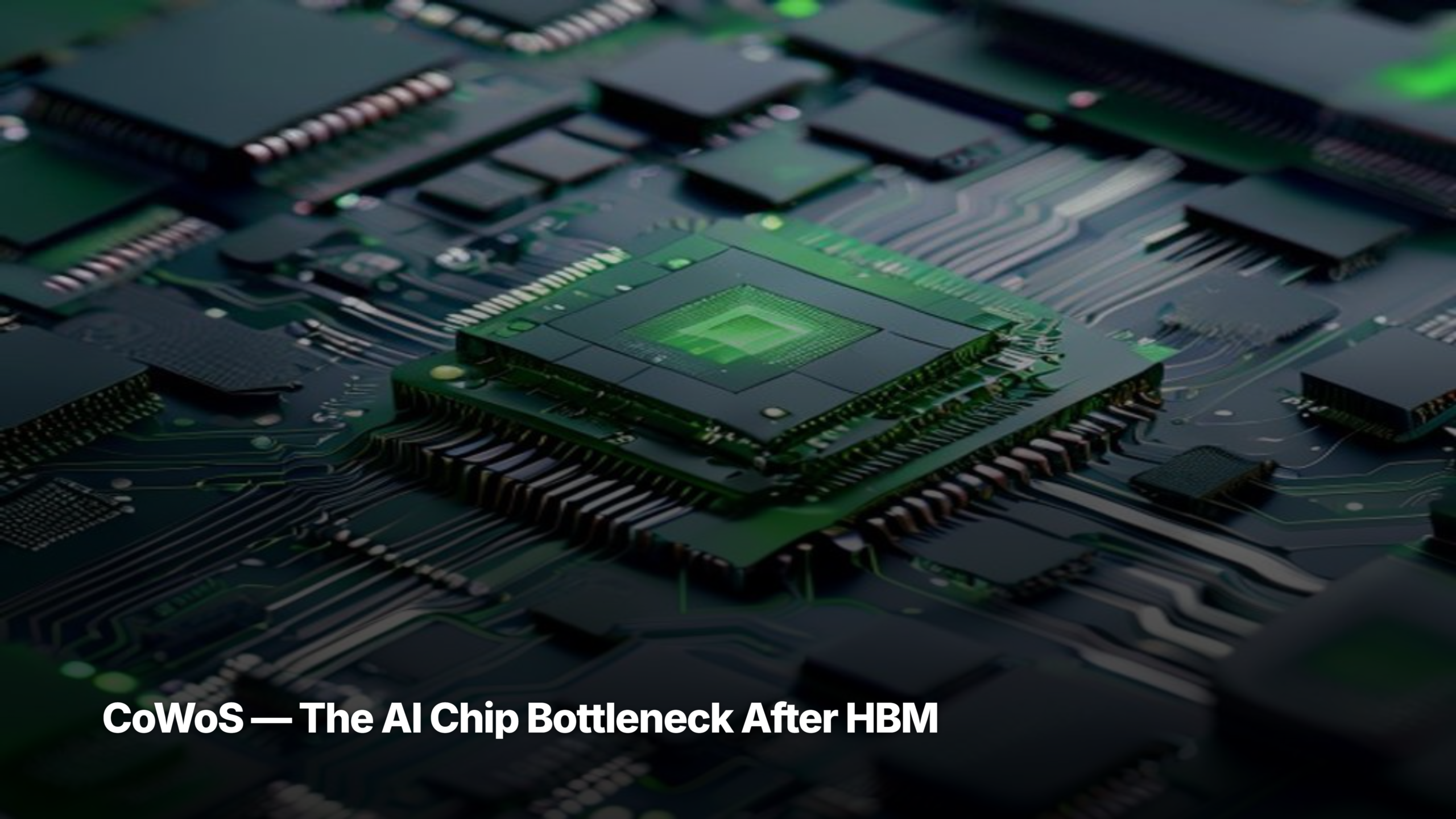
- CoWoS is TSMC's advanced packaging step — it bonds the GPU die and HBM stacks onto a single silicon interposer; every Blackwell, MI300/MI350, Google TPU, AWS Trainium, and AVGO/MRVL custom AI chip routes through it.
- CoWoS capacity has ramped from ~15K wafers/month (end 2023) to ~75-80K (end 2025), and TSMC is targeting ~120-130K by late 2026 — yet the lines are still booked out more than 18 months forward.
- The investable leverage isn't only NVDA. It's TSM (the gatekeeper), the packaging-tool cohort (AMAT, KLAC, ASML), and the custom-silicon enablers (AVGO, MRVL) that share CoWoS allocation alongside NVDA.
The CoWoS packaging shortage is the constraint that decides which AI chips can ship in 2026 and which slip to 2027. Every Blackwell B100 needs one CoWoS slot. Every AMD MI300X needs one. Every Google TPU v7, AWS Trainium 3, Microsoft Maia 200, Meta MTIA v2, and Broadcom or Marvell custom AI ASIC routes through the same packaging line at one company: TSMC. CoWoS — Chip-on-Wafer-on-Substrate — is the 2.5D packaging step that took TSMC 12 years to commercialise and now gates the entire AI infrastructure cycle. Capacity is booked out more than two years forward. TSMC is roughly doubling capacity again in 2026, and it is still short of demand. The HBM shortage gets the press. CoWoS is the one immediately downstream — and the investor leverage doesn’t sit where most retail expects.
TSMC — ticker TSM — last traded at $385.48 going into publication on May 20, 2026, and has roughly doubled in the trailing twelve months. The chart matters less than the order book. Advanced packaging is the segment that has consumed the bulk of TSMC’s incremental capex through this cycle, and the demand curve in 2026 still runs ahead of the capacity ramp.
Why the CoWoS packaging shortage matters right now
The math is brutal. Each Blackwell B100 needs one CoWoS-L slot. TSMC’s stated capacity ramp: ~15,000 wafers/month at end of 2023, ~35,000 at end of 2024, ~75-80,000 at end of 2025, and a target of ~120-130,000 by late 2026 — roughly an 8-9× expansion over 36 months. Even at 130,000 wafers/month, projected demand from NVDA, AMD, and the AVGO/MRVL custom-silicon cohort runs ahead of supply through 2027.
Allocation is the new pricing. Customers don’t pay a CoWoS market price — they receive an allocation. TSMC’s own next-gen CoWoS roadmap and Morgan Stanley’s most recent industry tracker put NVDA’s share of 2026 CoWoS demand at roughly 60% (around 595,000 wafers in total demand, with ~510,000 of those slots booked at TSMC; the rest moves to OSAT partners as they bring up CoWoS-like capacity). AMD takes another 10-15%. AVGO and MRVL custom silicon — for Google, Meta, Microsoft, and Amazon — eats most of the remainder. A startup AI chip vendor without an existing TSMC relationship gets nothing.
This is why the 2026 hyperscaler capex cycle matters so directly. Microsoft, Google, Meta, and Amazon now guide to roughly $700 billion in combined capex for the year — Amazon ~$200B, Google ~$190B, Microsoft ~$190B, and Meta $125-145B per the latest company guidance. Roughly 75% of that is tied to AI infrastructure. The capex commentary translates almost directly into CoWoS slot demand. When a hyperscaler raises capex by $20 billion at the margin, the binding constraint between “we’d like to ship more GPUs” and “we can actually ship them” is CoWoS.
And the lead times don’t help. Building a new CoWoS line from greenlight to volume takes 18 to 24 months — cleanroom construction, hybrid bonders, advanced lithography for the interposer wafers, technician training, and yield ramp. TSMC has recently compressed that to 1.5-2 years, but compressed is still slow relative to a hyperscaler capex cycle that re-rates every quarter. TSMC can’t simply spin up capacity in response to one quarter’s demand surge — even when its customers are pre-paying for slots.
How CoWoS actually works
“Chip-on-Wafer-on-Substrate” is a literal description of the stack. Chip dies are first bonded onto a silicon wafer — the “interposer”. That wafer is then mounted on a larger organic substrate, which becomes the package. Three layers — hence the “2.5D” label that sits between traditional 2D side-by-side packaging and full 3D die stacking.
The interposer is the secret. It’s a thin silicon wafer — roughly 100 microns thick — with thousands of micro-traces and through-silicon vias (TSVs) running across it. The GPU die sits in the middle of the interposer. HBM stacks sit on either side. The interposer provides the ultra-short, ultra-dense connections — more than 10,000 traces — needed to support HBM’s terabyte-per-second memory bandwidth. An ordinary PCB substrate cannot physically support that interconnect density at the pitch the silicon requires. We covered the memory side of this equation in our deep dive on HBM memory — CoWoS is the packaging step immediately downstream of those HBM stacks.
TSMC ships three flavours of CoWoS, and they are not interchangeable:
- CoWoS-S (Silicon interposer) — the original, used through H100. Gen-1 was limited to roughly 1.5× reticle size (~830 mm²). Current Gen-5 supports up to 3.3× reticle (~2,700 mm²). Mature and high-yield, but the silicon interposer cost scales with area.
- CoWoS-L (Local Silicon Interconnect plus organic redistribution) — what Blackwell B100, AMD MI350, and most 2026-vintage AI chips use. Starts at 1.5× reticle with one SoC plus four HBM cubes, and scales further. TSMC’s “Super Carrier” roadmap targets 9-14× reticle by 2027-29 to support 12-24 HBM4/HBM5E stacks per package. The 2026 capacity expansion is overwhelmingly CoWoS-L.
- CoWoS-R (RDL interposer) — newest variant, uses organic redistribution layers rather than a full silicon interposer. Lower interconnect density than CoWoS-L but cheaper; targeted at AI ASICs and mid-range accelerators where the silicon interposer is overkill.
Once a GPU die comes off TSMC’s N3 or N4 logic line and HBM stacks arrive from SK Hynix, Micron, or Samsung, the packaging steps are roughly: wafer probe and known-good-die test; die singulation; interposer fabrication on a silicon wafer using older-node lithography (the KrF and i-line tools, where ASML still sells); hybrid bonding of the dies to the interposer (Applied Materials, BESI, and Disco tools); encapsulation and molding; bonding of the wafer-level package onto the substrate; and final test, with KLA optical and e-beam metrology running through every step.
And this is why TSMC has the dominant share. Samsung’s I-Cube, Intel’s Foveros, and ASE’s SoIC are credible technologies on paper — structurally peer. They are behind on volume and yield at the AI-chip node where it matters. Hybrid bonding at sub-10-micron pitch is hard. TSMC has a 12-year head start, the customer relationships built over that period, and reportedly 98%+ CoWoS yield at AI-chip volumes. Customers exploring multi-sourcing — Amazon and Google have both kicked the tires on alternatives — typically end up using TSMC CoWoS for their highest-end SKU and routing mid-tier silicon through the alternatives.
Where the money flows
Cross the supply chain from gatekeeper to demand-side and the names sort into four buckets — only the last one is already well-priced.
The gatekeeper. TSM has the dominant share of high-end AI-chip CoWoS — NVDA alone has booked roughly 60% of the company’s 2026 capacity per Morgan Stanley’s industry tracker. Advanced packaging (CoWoS-dominated) is around 10% of TSMC’s revenue today, its highest-margin and fastest-growing segment; management has pointed publicly to advanced packaging becoming a much larger share long-term. CoWoS wafer ASPs are reported to be approaching the price of TSMC’s 7nm logic wafers, and they only have one direction while allocation remains rationed.
The packaging-tool cohort — the picks-and-shovels play. This is the bucket retail underweights because it sits one layer removed from the GPU headline.
- Applied Materials (AMAT) sells the deposition and etch tools that build the silicon interposer wafer, plus a growing share of the hybrid bonding equipment. Its Semiconductor Systems segment has flagged advanced packaging as the fastest-growing tool category in earnings commentary.
- KLA Corp (KLAC) sells the optical and e-beam metrology used to inspect interposer wafers, bumps, and bond integrity at each step. Packaging metrology has shifted from “afterthought” to “non-negotiable” because AI chip yields can’t tolerate post-packaging defects.
- ASML Holding (ASML) ships the KrF and ArF lithography systems used on the interposer wafers themselves — not the EUV machines that print the logic die, but the older-node lithography that ASML still sells and supports profitably.
- Lam Research (LRCX) covers etch and deposition tools for TSVs and bumping — smaller direct CoWoS exposure than AMAT or KLAC, but in the cohort.
- FormFactor (FORM) makes wafer probe cards used in HBM and CoWoS test. Smaller cap, more concentrated exposure than the big three.
The custom-silicon enablers — the second-order play.
- Broadcom (AVGO) is the custom AI ASIC partner for Google’s TPU silicon, with a fifth XPU customer added in late FY25. Every Broadcom custom AI chip routes through TSMC CoWoS. AVGO’s AI-semiconductor revenue hit $6.5 billion in Q4 FY25 alone — roughly $26 billion annualised at that pace — and Q1 FY26 is guided at $8.2 billion per the most recent Form 8-K filing. The AI order backlog stands near $73 billion per the latest disclosure, which extends well into 2027. That backlog is, in effect, pre-booked CoWoS capacity.
- Marvell Technology (MRVL) is the custom silicon partner for AWS Trainium and other hyperscaler ASIC programs. Same CoWoS-routed exposure as AVGO, smaller AI run-rate.
The demand-side names — already well-priced.
- NVDA is the primary CoWoS consumer. Obvious. The exposure is already in most portfolios — and at ~60% of 2026 CoWoS allocation, NVDA is the company whose shipment volumes are most directly capped by TSMC’s packaging ramp.
- AMD takes the MI300/MI350 share of CoWoS — growing, but a fraction of NVDA’s slot count.
The retail-investor takeaway is structural: if AI infrastructure exposure is 100% NVDA, the packaging-tool cohort (AMAT, KLAC, ASML) and the custom-silicon names (AVGO, MRVL) are leveraged to the same capex cycle from a less crowded starting point. CoWoS is the bottleneck. The leverage to that bottleneck sits with the gatekeeper and the tool suppliers, not only with the chip designers. Readers who track institutional positioning in semiconductor ETFs (SOXX, SMH) tend to see this rotation move first.
What could break this thesis
The bull case on CoWoS is consensus — which is exactly why it’s worth naming the things that could break it.
TSMC capacity catches up faster than demand. The 8-9× ramp from 2023 to 2026 is the most aggressive packaging expansion in semiconductor history. If hyperscaler AI capex pauses — and the 75% AI share of that $700B is the variable to watch — CoWoS could go from “sold out” to “balanced” within two quarters. Packaging margins compress quickly when allocation tension breaks.
Samsung or Intel closes the gap. Both have technically-peer offerings. If even one closes within an 18-month window, TSMC’s monopoly-grade pricing power erodes. Apple, Google, and Amazon have all publicly explored multi-sourcing the highest-volume nodes.
Chiplet alternatives via UCIe. The Universal Chiplet Interconnect Express standard lets you connect smaller dies on a cheaper organic substrate without a silicon interposer. If the industry standardises on organic chiplet packaging for inference workloads, CoWoS demand bifurcates — high-end training stays on CoWoS, high-volume inference moves to organic — and TSMC’s CoWoS share of total AI packaging compresses, even as the TAM grows.
HBM4 architecture shifts. HBM4, shipping in volume from late 2026, may use hybrid bonding directly to the GPU die rather than via an interposer. The packaging step still happens at TSMC, but the CoWoS-L variant specifically could plateau if the industry pivots to true 3D stacking faster than expected.
China export controls extend to packaging. US restrictions currently focus on logic process nodes. If advanced packaging is added to the export-control entity list, the TAM bifurcates and the Chinese AI buildout funds domestic packaging alternatives (CXMT, JCET). Less likely than the other risks — but the highest-velocity one if it lands.
What to watch
The CoWoS thesis is trackable from public disclosures alone.
- TSMC quarterly capacity guidance. Every TSMC earnings call references advanced packaging in management Q&A. The wafers/month run-rate vs. the prior quarter is the cleanest read on whether the 130K target for end of 2026 is on track.
- AMAT and KLAC earnings commentary. Advanced packaging is now broken out — or addressed directly — in Semiconductor Systems and Wafer Inspection segment commentary. Watch for orders-from-foundry colour each quarter.
- AVGO and MRVL AI revenue prints. A clean proxy for the custom-silicon share of CoWoS allocation against NVDA. The AVGO backlog at $73B is forward CoWoS demand, locked in.
- TrendForce and DigiTimes monthly packaging trackers. Industry data on CoWoS share-of-capacity by customer, updated more frequently than the quarterly earnings cycle. Often the first place a slip in NVDA’s allocation share shows up.
- HBM4 ramp milestones. Late-2026 production milestones at SK Hynix, Micron, and Samsung will tell you whether packaging architecture continues to favour CoWoS-L or starts shifting toward true 3D stacking — which would re-rate the CoWoS-L specific bull case.
The HBM shortage gets the headlines. CoWoS is the choke point one step downstream — quieter, more concentrated, and the place where the AI capex cycle ultimately hits a physical constraint. The names that benefit aren’t only the ones on the front of every retail brokerage app. If you already own a semiconductor index, you own a slice of this; if you’re tracking how a semis ETF actually weights its holdings, the packaging-tool cohort is the under-represented bucket. The supply chain doesn’t care about narrative. It cares about wafer slots.
Get early access to Orbit
Orbit is Luna3.ai’s AI-augmented research engine. 12 algorithmic signals + a gradient-boosted ML model + an agentic LLM that reads each top pick’s filings and writes a daily thesis with conviction score and catalyst proximity. Three regimes, three playbooks — growth in expansion, defensives in late-cycle, recovery plays at panic bottoms. The 3 in Luna3.ai.
No spam. Unsubscribe any time.
No comments yet. Be the first to share your thoughts!